Home>diy>Architecture & Design>How To Use Eagle CAD
Architecture & Design
How To Use Eagle CAD
Modified: September 1, 2024
Learn how to efficiently use Eagle CAD for architecture design projects with our comprehensive guide and expert tips. Enhance your design process and create stunning projects.
(Many of the links in this article redirect to a specific reviewed product. Your purchase of these products through affiliate links helps to generate commission for Storables.com, at no extra cost. Learn more)
Introduction
When it comes to designing electronic circuits and printed circuit boards (PCBs), having the right software can make all the difference. Eagle CAD (Computer-Aided Design) is one such software, widely used in the industry for its powerful features and user-friendly interface. Whether you’re a professional engineer or a hobbyist, learning how to use Eagle CAD can greatly enhance your ability to create and optimize electronic designs.
In this article, we will guide you through the process of using Eagle CAD, from installation to generating Gerber files for manufacturing. We will cover everything from creating schematics to designing custom PCB layouts, giving you the necessary knowledge and skills to bring your electronic projects to life.
Getting started with Eagle CAD may seem daunting at first, especially if you’re new to CAD software. But fear not! With a little practice and guidance, you’ll soon become familiar with Eagle’s interface and be able to leverage its extensive functionality.
Before diving into the details of using Eagle CAD, it’s important to understand its purpose and advantages. Eagle CAD is an industry-standard software tool for designing circuit schematics and PCB layouts. It offers a comprehensive suite of features that facilitate the entire design process, from creating the initial schematic to generating output files for manufacturing.
One of the key benefits of using Eagle CAD is its flexibility and scalability. Whether you’re working on a simple circuit or a complex multi-layered PCB, Eagle CAD has the tools to handle it all. It supports both single-layer and multi-layer PCB designs, allowing you to choose the most appropriate option for your project.
Another advantage of Eagle CAD is its extensive library of electronic components. The software comes with a vast collection of pre-built component libraries, ranging from common resistors and capacitors to specialized ICs and connectors. This library saves you time and effort by providing ready-to-use component symbols and footprints, eliminating the need to create them from scratch.
Furthermore, Eagle CAD offers a comprehensive set of design validation and verification tools. These tools help ensure your design meets all the necessary electrical and physical requirements. For example, the Design Rule Check (DRC) feature checks for common design errors, such as spacing violations and overlapping traces. This greatly reduces the risk of manufacturing defects and improves the overall quality of your design.
In the next sections of this article, we will guide you through the process of installing Eagle CAD, creating schematics, designing PCB layouts, and generating Gerber files for manufacturing. So, let’s get started with exploring the world of Eagle CAD!
Key Takeaways:
- Eagle CAD is a powerful and user-friendly software for PCB design, offering a seamless process from installation to generating Gerber files. Its comprehensive features and functionalities cater to both professionals and hobbyists, enabling the creation of innovative electronic projects.
- The PCB design process in Eagle CAD involves critical steps such as setting up the board layout, placing components, routing traces, performing a Design Rule Check (DRC), and generating Gerber files. Thorough attention to detail and adherence to best practices ensure a successful and reliable PCB design.
Read more: What Is CAD Used For
Getting Started
Before you can start using Eagle CAD, you need to ensure that you have the software installed on your computer. Fortunately, Eagle CAD is available for both Windows and Mac operating systems, making it accessible to a wide range of users.
To install Eagle CAD, you can visit the official Autodesk website and download the latest version of the software. Once downloaded, run the installer and follow the on-screen instructions to complete the installation process.
After installation, launch Eagle CAD from your desktop or start menu. The first time you open Eagle CAD, you will be prompted to sign in using your Autodesk account. If you don’t have an account, you can create one for free.
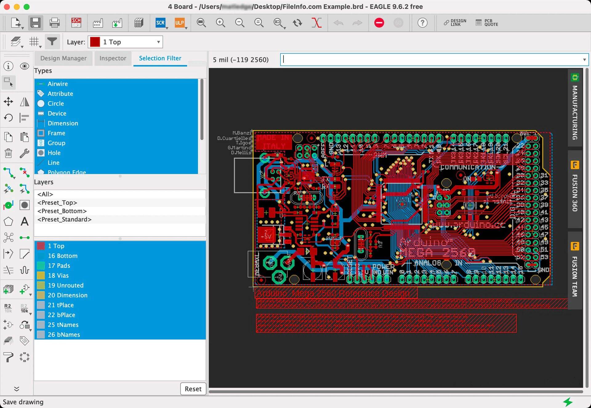
Once you’re signed in, you’ll be greeted by the Eagle CAD user interface. The interface is divided into several panels, each serving a specific purpose. The main panels include the Schematic Editor, Layout Editor, Library Editor, and Design Manager.
Before you jump into creating a new project, it’s helpful to familiarize yourself with the main components of the Eagle CAD interface. The Schematic Editor is where you’ll create and edit the circuit schematics. The Layout Editor is where you’ll design the physical layout of the PCB. The Library Editor is where you’ll manage and create component libraries. And finally, the Design Manager is where you’ll organize and manage all your project files.
Now that you understand the basics of the Eagle CAD interface, let’s move on to creating your first project. Click on the “File” menu and select “New Project” from the dropdown menu. Give your project a name and specify the location where you want to save it. Click “Save” to create the project.
With your project created, you’re ready to start designing schematics or PCB layouts. To create a new schematic, click on the “File” menu and select “New” followed by “Schematic.” This will open a blank schematic sheet where you can begin designing your circuit.
If you prefer to start by designing the PCB layout, you can click on the “File” menu and select “New” followed by “Board.” This will open a blank PCB layout where you can place and route components.
Now that you have a basic understanding of how to get started with Eagle CAD, you’re ready to dive into the specifics of creating schematics, designing PCB layouts, and utilizing the various features of the software. In the next sections, we’ll explore each step in detail, guiding you through the process from start to finish.
Don’t worry if it takes a little time to get comfortable with Eagle CAD. Like any new software, it takes practice and exploration to fully grasp its capabilities. With time and patience, you’ll become a proficient user and be able to harness the power of Eagle CAD for your electronic design projects.
Installing Eagle CAD
Installing Eagle CAD on your computer is a straightforward process that can be done in a few simple steps. By following these steps, you’ll have Eagle CAD up and running in no time.
The first step is to visit the official Autodesk website and navigate to the Eagle CAD download page. Here, you’ll find the latest version of the software available for both Windows and Mac operating systems. Choose the version that is compatible with your operating system and click on the download button.
Once the download is complete, locate the installer file in your downloads folder or wherever your browser saves downloaded files. Double-click on the installer file to begin the installation process.
Follow the on-screen instructions provided by the installer. You will be prompted to accept the software license agreement. Read through the terms and conditions and click on the “Agree” or “Accept” button to proceed.
Next, you’ll be asked to choose the installation location for Eagle CAD. The default location is usually in the “Program Files” or “Applications” folder. If you would like to change the location, click on the “Browse” button and select a different folder. Once you’ve chosen the installation location, click on the “Next” button.
After selecting the installation location, you may be given the option to choose additional components to install. These components include libraries, example projects, and documentation. You can choose to install these components for additional resources and examples or leave them unchecked if you prefer not to install them. Click on the “Next” button to proceed.
At this point, the installer will begin copying the necessary files to your computer. The process may take a few minutes, depending on the speed of your computer. Once the installation is complete, you’ll see a confirmation message indicating that Eagle CAD has been successfully installed.
With Eagle CAD now installed on your computer, you can launch the program and begin exploring its features and functionalities. You may be prompted to sign in using your Autodesk account, or create a new account if you don’t have one already.
By following these steps, you’ve successfully installed Eagle CAD on your computer. Now, you’re ready to start designing schematics and PCB layouts, and taking advantage of the powerful tools and capabilities that Eagle CAD offers.
Keep in mind that periodically checking for software updates is also important to ensure that you’re using the latest version of Eagle CAD. Updates often include bug fixes, new features, and improved performance, so staying up to date is recommended.
Now that you have Eagle CAD installed, let’s move on to the next step: opening a new project and getting started with the design process.
Opening a New Project
Once you have Eagle CAD installed on your computer, it’s time to start working on your first project. Opening a new project in Eagle CAD is a simple process that provides you with a blank canvas to begin your design.
To open a new project in Eagle CAD, follow these steps:
- Launch Eagle CAD from your desktop or start menu.
- When the application opens, you’ll be greeted by the Eagle CAD Control Panel.
- In the Control Panel, click on the “New” button located in the upper left corner. This will open the New Project dialog box.
- In the New Project dialog box, enter a name for your project in the “Name” field. Choose a name that is descriptive and easily identifiable.
- Specify the location where you want to save your project in the “Location” field. You can use the default location or browse to a specific folder on your computer.
- Click on the “OK” button to create the new project.
Once you’ve created the new project, you’ll see the Eagle CAD interface with the Design Manager panel open. The Design Manager panel displays all the files associated with your project, including schematics, layouts, libraries, and other project-related files.
From the Design Manager panel, you can navigate through your project files, open existing files, and create new files. If you’re starting a new project, this panel will be empty except for the default project file that was automatically created when you created the project.
To create a new schematic or PCB layout within your project:
- Click on the “File” menu in the Eagle CAD menu bar.
- Select “New” and choose either “Schematic” or “Board” depending on which type of file you want to create.
- A new blank schematic or board file will open, and you can begin your design by adding components, wiring connections, and creating your circuit.
Opening a new project in Eagle CAD is a crucial first step in the design process. It provides you with a dedicated space to organize and manage all your project files, ensuring that your work stays organized and easily accessible.
Remember to save your project regularly to safeguard your progress. Eagle CAD allows you to save your work in the .sch format for schematics and the .brd format for board layouts. Saving your work ensures that no progress is lost in case of unexpected disruptions or computer malfunctions.
Now that you know how to open a new project in Eagle CAD, let’s move on to creating schematics and introducing components into your design.
Creating Schematics
Schematics are the foundation of any electronic design, serving as a visual representation of how components are connected in a circuit. In Eagle CAD, creating schematics is a crucial step towards designing your electronic project.
To create a new schematic in Eagle CAD, follow these steps:
- Ensure that an open project is available in the Design Manager.
- Click on the “File” menu in the Eagle CAD menu bar.
- Select “New” and choose “Schematic”.
- A new blank schematic sheet will open, ready for you to start designing your circuit.
Once you have a blank schematic in front of you, it’s time to begin adding components and creating connections. Here’s how:
- Click on the “Library” menu in the Eagle CAD menu bar and select “Use” to open the Library Manager.
- In the Library Manager, you can search and select the library containing the components you need for your circuit. If you have downloaded custom component libraries, click on the “Add” button to add them to the list of available libraries.
- Once the desired library is selected, click on the “OK” button to close the Library Manager.
- In the schematic sheet, click on the “Add” button located in the left toolbar or press the “A” keyboard shortcut.
- A dialog box will appear, displaying the components available in the selected library. Browse or search for the component you want to add, select it, and click on the “OK” button.
- The selected component will appear as a crosshair cursor on the schematic sheet. Click on the desired location to place the component on the sheet.
- Repeat the process to add additional components to your schematic. Connect component pins by clicking on one pin and dragging the wire to the other pin or junction. Use the “Net” tool to name the connections.
As you add components and create connections, it’s important to pay attention to the organization and clarity of your schematic. Keep related components closer to each other and use logical wiring patterns to improve readability. Proper labeling and naming of components and nets will also help with clarity and reduce confusion during the design process.
Eagle CAD provides additional features and functionality to enhance the schematic creation process. For example, you can add text annotations, draw lines and shapes, and even include graphical images as part of your schematic design.
Another useful tool is the “ERC” (Electrical Rule Check), which helps identify potential electrical errors in your schematic design. Running the ERC ensures that you haven’t made any mistakes such as shorted connections or incorrectly wired components.
Once you have finished creating your schematic, it’s important to save your work. Use the “File” menu and select “Save” or press the “Ctrl + S” keyboard shortcut to save your progress.
Creating schematics in Eagle CAD allows you to visually represent your circuit design and serves as a blueprint for further steps in the electronic design process. With components added and connections made, you’re now ready to move on to the next stage: placing components on the PCB layout.
Read more: How Is CAD Used In Engineering
Placing Components
After creating a schematic in Eagle CAD, the next step in the electronic design process is to place components on the PCB (Printed Circuit Board) layout. Placing components accurately and thoughtfully on the PCB is crucial for the successful assembly and functionality of your electronic project.
To place components on the PCB layout in Eagle CAD, follow these steps:
- Open the PCB layout by clicking on the “File” menu in the Eagle CAD menu bar and selecting “New” followed by “Board”.
- You will be presented with a blank PCB layout canvas.
- In the Design Manager, locate the schematic associated with your PCB layout.
- Drag and drop the schematic onto the PCB layout canvas. This action will automatically populate the PCB layout with the components from the schematic.
At this point, you will see all the components from the schematic appear on the PCB layout canvas, but they will be scattered randomly. To properly place the components, you can follow these best practices:
- Ensure that there is sufficient space between components to allow for proper routing of traces and clearance for soldering during assembly.
- Consider the schematic design and group associated components closer to each other on the PCB layout. This helps with trace routing and reduces signal interference.
- Align components based on functionality or logical groupings to improve the overall aesthetics and organization of the PCB layout.
- Take into account any mechanical constraints or mounting requirements when placing components. Ensure there is enough clearance for connectors, mounting holes, and other physical elements of the project.
Eagle CAD provides several tools to help you place components accurately and precisely on the PCB layout. The “Move” tool allows you to select and move components around the canvas. You can use the “Rotate” tool to change the orientation of components as needed.
Keep in mind that certain components may need to be rotated or flipped to match their correct orientation on the PCB layout. Some components, such as polarized capacitors or diodes, have specific pin orientations that must be followed. Double-check the datasheets or component footprints to ensure correct placement and orientation.
Eagle CAD also provides automatic component placement features, such as the “Auto-Placement” tool. This tool can help you quickly arrange components on the PCB based on predefined rules and constraints, saving you time and effort in the placement process.
Throughout the component placement process, it’s essential to regularly save your progress to prevent any data loss. Use the “File” menu and select “Save” or use the “Ctrl + S” keyboard shortcut to save your work.
By carefully placing components on the PCB layout in Eagle CAD, you lay the groundwork for the next step: routing the PCB traces. Proper component placement ensures efficient signal flow, reduces signal interference, and allows for easier assembly and manufacturing of the PCB.
In the next section, we will explore the process of routing the traces on the PCB layout to ensure electrical connections between components.
Wiring Connections
After placing components on the PCB layout in Eagle CAD, the next step is to wire the connections between the components. Wiring the connections ensures that electrical signals can flow through the circuit and enables proper functionality of your electronic project.
To wire connections between components in Eagle CAD, follow these steps:
- Ensure that you have the PCB layout open in the Eagle CAD interface.
- Review the schematic to understand how the components are connected and which pins need to be wired together.
- Click on the “Route” button in the toolbar or press the “R” key on your keyboard to activate the routing mode.
- Select the desired layer for routing by clicking on the appropriate layer button in the layer selection toolbar. The default is usually the top layer, but you can switch to the bottom layer or any other available layer as needed.
- Start routing by clicking on a pin or pad of a component. Then, click on the destination pin or pad of the component you want to connect.
- Eagle CAD will automatically create a trace between the two points, following the shortest route available while adhering to the design rules you have set.
- Continue routing by clicking on additional pins or pads and connecting them to their appropriate destinations.
- If you need to change layers during the routing process, use the “Change Layer” button or the “Shift + Wheel” shortcut to move between layers.
While routing the connections, it’s important to follow good PCB design practices to ensure optimal performance and reliability of your circuit. Here are some tips to consider:
- Keep wire lengths as short as possible to minimize signal degradation and electromagnetic interference.
- Avoid crossing traces unless necessary. If crossing is inevitable, use vias and proper clearance to prevent signal interference.
- Assign net labels to important connections to improve clarity and simplify debugging and future modifications.
- Ensure that there is sufficient clearance between traces and adjacent components or copper pours to minimize the risk of shorts or signal crosstalk.
- Use appropriate trace widths based on the current handling capacity and signal requirements to prevent excessive heat or signal loss.
- Take advantage of the “Ripup” tool to remove or modify existing traces when needed.
Eagle CAD provides Design Rule Check (DRC) functionality to ensure that your routing meets the necessary electrical and physical requirements. Running the DRC can help identify potential design errors, such as clearance violations, silkscreen overlap, or poorly placed components.
Regularly save your progress during the routing process to safeguard your work. Use the “File” menu and select “Save” or press the “Ctrl + S” keyboard shortcut.
Wiring connections in Eagle CAD is a crucial step in the PCB design process, as it brings your electronic circuit to life. With proper routing techniques and attention to detail, you will ensure the functionality and reliability of your electronic project.
In the next section, we will explore how to edit schematics and modify the component placement and wiring if necessary.
Editing Schematics
Editing schematics in Eagle CAD allows you to modify and refine your circuit design as you go through the electronic design process. Whether you want to add or remove components, change connections, or make adjustments to the overall circuit, Eagle CAD provides a range of tools and features to help you make these modifications.
To edit schematics in Eagle CAD, follow these steps:
- Open the schematic that you want to edit in Eagle CAD.
- Click on the “Edit” button in the toolbar or press the “E” key on your keyboard to activate the edit mode.
- Select the component or wire that you want to modify by clicking on it.
- Once selected, you can make various modifications, including moving components, changing component properties, deleting components or wires, and adding new components.
- Use the “Move” tool to relocate components within the schematic. Click and drag the component to a new position to reposition it.
- To change the properties of a component, select it and open the properties dialog box. Here, you can modify parameters such as the component value, reference designator, and footprint.
- To delete a component or wire, select it and press the “Delete” key on your keyboard. Alternatively, you can use the right-click menu and choose the “Delete” option.
- If you want to add new components, click on the “Add” button in the toolbar or press the “A” key on your keyboard. Select the desired component from the available libraries and place it in the schematic.
- Make any other necessary modifications to the schematic to meet your design requirements.
Editing schematics in Eagle CAD allows you to refine your circuit design based on feedback or new design considerations. It gives you the flexibility to adjust component placement, optimize connections, and improve the overall functionality and clarity of your circuit.
During the editing process, it’s important to keep track of any changes made and ensure that they align with your design goals. Proper organization and labeling of components, nets, and design elements will help maintain the integrity of your schematic.
Remember to regularly save your progress while editing the schematic. Use the “File” menu and select “Save” or press the “Ctrl + S” keyboard shortcut.
In addition to modifying the schematic, you may also need to update the PCB layout to reflect any changes. In Eagle CAD, changes made in the schematic are not automatically reflected in the PCB layout. You will have to update the PCB layout manually by synchronizing the changes from the schematic.
To synchronize the changes from the schematic to the PCB layout:
- Open the PCB layout associated with your schematic.
- Click on the “File” menu and select “Update PCB” to update the PCB layout based on the changes made in the schematic.
Editing schematics in Eagle CAD is an iterative process that allows you to refine and optimize your circuit design. By leveraging the editing tools and features available, you can create a schematic that accurately represents your electronic project and meets your design objectives.
In the next section, we will delve into designing and setting up the board layout for your PCB.
Designing Printed Circuit Boards (PCBs)
Designing a printed circuit board (PCB) is a critical step in the electronic design process. A well-designed PCB layout ensures the proper functioning and reliability of your electronic project. In Eagle CAD, you have a range of tools and features available to help you design and optimize your PCB layout.
To begin designing a PCB layout in Eagle CAD, follow these steps:
- Open the schematic associated with your PCB layout in Eagle CAD.
- Click on the “File” menu and select “Switch to Board” to switch from the schematic to the PCB layout.
- You will be presented with a blank PCB layout canvas, ready for you to start designing.
Designing a PCB layout involves several key steps, including setting up the board layout, placing components, routing traces, and performing design checks. Let’s explore each step in more detail:
Read more: Why Do We Use CAD
Setting Up the Board Layout
Before you start placing components and routing traces, it’s important to set up the board layout properly. Here are some key considerations:
- Choose the appropriate board size and shape, considering any mechanical constraints or housing requirements.
- Define the layer stack-up, specifying the number of layers and their order (top, inner, bottom).
- Set up design rules, including trace width, clearance, and minimum drill sizes.
- Define any copper pours or planes, such as ground or power planes, for improved signal integrity and noise reduction.
Placing Components on the PCB
Once the board layout is set up, it’s time to place the components on the PCB. Here are some tips for efficient component placement:
- Consider the schematic design and group related components closer to each other.
- Ensure there is sufficient space between components for traces and proper clearance for assembly.
- Take into account any mechanical constraints or mounting requirements.
- Arrange components to minimize signal interference and optimize signal flow.
Routing the PCB
With components placed on the PCB, you can start routing the traces to establish electrical connections. Some tips for effective trace routing include:
- Keep traces as short as possible to minimize signal degradation and EMI (electromagnetic interference).
- Avoid crossing traces unless necessary, and use vias and appropriate clearance to prevent signal interference.
- Assign net labels and use color-coding to improve clarity and simplify debugging.
- Adhere to design rules, such as trace width and clearance, to ensure proper signal integrity.
Performing Design Rule Checks (DRC)
Once the routing is complete, it’s essential to perform a Design Rule Check (DRC) to identify and rectify any design errors or violations. The DRC ensures that your PCB layout meets electrical and physical requirements, such as clearance violations, overlapping traces, or component spacing.
Read more: How To Use AutoCAD For Landscape Design
Generating Gerber Files
To get your PCB manufactured, you will need to generate Gerber files, which are standard file formats used by PCB manufacturers. Eagle CAD provides tools to generate these files, allowing you to export the necessary data for fabrication.
Throughout the PCB design process, it’s important to save your progress regularly to prevent any data loss. Use the “File” menu and select “Save” or press the “Ctrl + S” keyboard shortcut to save your work.
Designing a PCB layout can be a complex task, but with the right tools and knowledge, you can create a well-optimized and functional layout. By following best practices and leveraging the features of Eagle CAD, you’ll be on your way to a successful PCB design.
In the next section, we will dive deeper into each step of the PCB layout process, providing you with detailed guidance and insights to help you create professional-quality PCB designs.
Setting Up the Board Layout
Setting up the board layout is a critical step in designing a printed circuit board (PCB) using Eagle CAD. Properly configuring the board layout ensures the functionality, manufacturability, and reliability of your electronic project. Here are the key considerations when setting up the board layout:
Board Size and Shape
Begin by determining the size and shape of the PCB. Consider any mechanical constraints, such as the available space within an enclosure or mounting requirements. Ensure that the dimensions and shape of the PCB are compatible with your project’s needs and intended application.
Layer Stack-up
Evaluate the complexity and requirements of your design to determine the layer stack-up. The stack-up defines the number of layers in the PCB and their order (top, inner, bottom). Consider factors such as signal integrity, power distribution, and noise management. Multi-layer PCBs provide more flexibility for routing complex circuits, but come with added cost and fabrication complexity.
Read more: How Do CAD Engineers Use Geometry
Design Rules
Define the design rules that govern your PCB layout. These rules include parameters such as trace width, clearance, and minimum drill sizes. Consider the capabilities of your manufacturer and the requirements of your components when setting these rules. Adhering to design rules ensures proper signal integrity, manufacturability, and reliability.
Copper Pours or Planes
Determine whether you need to incorporate copper pours or planes into your PCB layout. Copper pours are large areas of copper on the PCB used for ground planes, power planes, or signal shielding. These planes provide improved signal integrity, noise reduction, and thermal dissipation. Define the shape, size, and location of these copper pours based on the specific design requirements.
Eagle CAD provides the necessary tools to set up the board layout effectively. You can access these tools through the main top menu and the properties dialog boxes. Take your time to explore and adjust the settings to match your specific design requirements.
During the board layout setup, it’s crucial to consider factors such as signal integrity, thermal management, and manufacturability. By carefully configuring the board layout, you pave the way for a successful and reliable PCB design.
Remember to regularly save your progress while setting up the board layout. Use the “File” menu and select “Save” or press the “Ctrl + S” keyboard shortcut to save your work.
Now that you have set up the board layout, you can proceed to placing components on the PCB and routing the necessary connections. These steps, which we will explore in the following sections, bring your design closer to completion and manufacturing.
Placing Components on the PCB
Placing components on the printed circuit board (PCB) is a crucial step in the design process. Proper component placement ensures efficient signal flow, optimal trace routing, and facilitates ease of assembly and manufacturing. Here are some key considerations when placing components on the PCB in Eagle CAD:
Consider the Schematic
Refer to the schematic to understand how components are interconnected and the logical grouping of related components. This will help you determine the most suitable placement arrangement on the PCB.
Read more: How Do Interior Designers Use CAD
Organize Components
Group related components together based on their functionality, proximity to each other on the schematic, or other design considerations. For example, place power-related components close to the power input, and place signal processing components in a dedicated area.
Space Considerations
Ensure that there is sufficient space between components to accommodate traces and vias. Leave room for proper clearance and soldering during assembly. Consider the physical dimensions of the components, their heat dissipation requirements, and any mechanical constraints specified for your project.
Orientation and Alignment
Take component orientation into account when placing them on the PCB. Ensure that polarized components, such as electrolytic capacitors or diodes, are correctly aligned. Align components in a neat and organized manner to improve the overall aesthetics and ease of trace routing.
Component Placement Strategies
There are various strategies you can employ when placing components on the PCB:
- Start with critical components: Begin by placing components that require specific placement, such as connectors or components with specific thermal requirements.
- Top-down placement: Place components from the top side of the PCB and work your way down towards the bottom layer, if applicable. This ensures smooth routing and avoids unnecessary crossovers.
- Grouping by function: Place components with similar functionality or those that interact closely together near each other to minimize trace length and signal interference.
- Use symmetry: If applicable, use component symmetry to maintain a balanced and visually appealing layout. This can also simplify routing and improve signal integrity.
- Consider signal flow: Place components in the direction of signal flow to minimize trace length, reduce transmission line effects, and ensure efficient signal propagation.
Eagle CAD provides several tools to assist you in component placement. Utilize features such as the “Move” tool to relocate components, the “Rotate” tool to adjust their orientation, and the “Group” function to manage related components collectively.
Remember to regularly save your progress while placing components on the PCB. Use the “File” menu and select “Save” or press the “Ctrl + S” keyboard shortcut to save your work.
By carefully placing components on the PCB in Eagle CAD, you set the foundation for smooth trace routing and ensure the overall performance and manufacturability of your electronic project.
Next, we’ll explore the process of routing the traces on the PCB layout to establish the necessary electrical connections.
Read more: How To Use FreeCAD To Design A House
Routing the PCB
Routing the printed circuit board (PCB) is a crucial step in the design process that involves creating the necessary electrical connections between components. By properly routing the traces, you ensure reliable signal flow, minimize electromagnetic interference (EMI), and enhance the performance of your electronic project. Here’s how to route traces on the PCB using Eagle CAD:
Activate the Routing Mode
Click on the “Route” button in the toolbar or press the “R” key on your keyboard to activate the routing mode in Eagle CAD. This allows you to create trace connections between the pins and pads of your components.
Select the Appropriate Layer
Choose the right layer for routing by clicking on the corresponding layer button in the layer selection toolbar. The default is usually the top layer, but you can switch to the bottom layer or any other available layer as needed.
Start Routing Traces
Begin routing traces by clicking on the starting point (pin or pad) of a component and then clicking on the destination point of the connection. Eagle CAD will automatically create a trace between the two points, following the shortest available route while adhering to the design rules you have set.
Read more: How To Design A House Plan Using AutoCAD
Route with Efficiency in Mind
When routing traces, keep the following considerations in mind:
- Keep traces as short as possible to minimize signal degradation and crosstalk.
- Avoid crossing traces unless necessary, and use vias and appropriate clearance to prevent interference.
- Maintain proper clearance between adjacent traces and nearby components to avoid electrical shorts.
- Ensure that traces are wide enough to carry the required current without overheating or voltage drop.
- Consider the signal integrity requirements of high-speed or sensitive signals, such as differential pairs or clock signals. Use proper routing techniques, such as length matching and impedance control, to maintain signal integrity.
Use the Autorouter (Optional)
Eagle CAD provides an autorouting capability as an option for automatically routing traces between components. However, manual routing is generally preferred for precise control over trace placement and adherence to design rules. Only consider using the autorouter for simple designs or as a starting point for further manual optimization.
Perform Design Rule Checks (DRC)
After completing the trace routing, run the Design Rule Check (DRC) feature in Eagle CAD. The DRC helps identify and rectify any design rule violations, such as clearance violations or overlapping traces. Address any errors or warnings raised by the DRC to ensure your PCB layout meets the required specifications.
Remember to save your progress regularly during the routing process. Use the “File” menu and select “Save” or press the “Ctrl + S” keyboard shortcut to save your work.
By carefully routing the traces on the PCB layout in Eagle CAD, you establish the necessary electrical connections, optimize signal flow, and ensure the overall functionality and performance of your electronic project.
In the next section, we’ll outline the process of performing a Design Rule Check (DRC) to identify and rectify any design errors or violations in your PCB layout.
Design Rule Check (DRC)
The Design Rule Check (DRC) is a critical step in the PCB design process that ensures your layout adheres to the necessary electrical and physical design rules. Running a DRC in Eagle CAD helps identify design errors, potential manufacturing issues, and violations that could affect the functionality and reliability of your printed circuit board (PCB).
Read more: How To Scale In CAD
Performing a DRC in Eagle CAD
Follow these steps to run a DRC in Eagle CAD:
- Ensure that you have completed the trace routing and are ready to validate your design.
- Click on the “Tools” menu in the Eagle CAD menu bar.
- Select “DRC” from the dropdown menu to open the Design Rule Check dialog box.
- In the Design Rule Check dialog box, you can set various parameters, including trace width, clearance, minimum drill size, and other design constraints specific to your project and manufacturer’s specifications.
- Once you have configured the DRC parameters, click on the “Run” button to perform the check.
- Eagle CAD will analyze your layout and report any design rule violations or errors.
- Review the DRC results to identify and understand the reported issues. Common violations include spacing violations, overlapping traces, unrouted connections, or incorrect pad sizes.
Addressing DRC Issues:
When the DRC detects violations or errors, it’s essential to address them to ensure a functional and manufacturable PCB. Here’s how to handle common DRC issues:
- Spacing violations: Adjust the spacing between traces, pads, and components to meet the minimum clearance defined by your design rules. This prevents potential electrical shorts or manufacturing issues.
- Overlapping traces: Reroute overlapping traces to eliminate any overlaps. Ensure that each trace has its dedicated space and does not interfere with neighboring traces.
- Unrouted connections: Review and complete any missing connections by routing the remaining traces to establish the required electrical connectivity.
- Pad size errors: Verify that the pad sizes match the footprint of the corresponding components. Adjust pad sizes as needed to ensure proper soldering and component placement.
Following a successful DRC, you can be confident that your PCB layout meets the necessary design rules and requirements. However, keep in mind that the DRC does not guarantee a flawless design. It is essential to thoroughly review your layout and perform additional checks to ensure the overall quality and functionality of your PCB design.
Regularly save your progress during the DRC process. Use the “File” menu and select “Save” or press the “Ctrl + S” keyboard shortcut to save your work.
By performing a Design Rule Check in Eagle CAD, you validate your PCB layout and ensure it conforms to electrical and physical design rules, reducing the risk of errors and manufacturing issues. With a successful DRC, you can proceed with generating the necessary files for manufacturing your PCB.
In the next section, we’ll explore the process of generating Gerber files for manufacturing your PCB design.
Generating Gerber Files
Generating Gerber files is a crucial step in the PCB design process as it provides the necessary data for manufacturing your printed circuit board (PCB). Gerber files are the industry-standard file format used by PCB manufacturers to manufacture and assemble PCBs accurately. To generate Gerber files in Eagle CAD, follow these steps:
Verify the Design
Before generating Gerber files, it’s essential to thoroughly review your PCB design, ensure that all connections and components are in the right place, and address any design rule violations identified during the Design Rule Check (DRC) process.
Click on the CAM Processor
In the Eagle CAD interface, click on the “CAM Processor” icon or access it through the “File” menu by selecting “CAM Processor” to open the CAM Processor dialog box. The CAM Processor is the tool used to generate the Gerber files.
Read more: What Does CAD Mean In TinkerCAD
Configure the Job
In the CAM Processor dialog box, create a new job by clicking on the “File” menu and selecting “New” or by clicking on the “New” button. Configure the job settings according to your manufacturer’s requirements.
Define the Output Settings
In the CAM Processor dialog box, select the layers you want to include in the Gerber files. Typically, these include top and bottom copper layers, silkscreen, solder mask, drill holes, and any other relevant layers. Verify that the correct layers are selected and adjust the settings if necessary.
Set the File Format and Output Location
In the CAM Processor dialog box, specify the output file format as Gerber (RS-274X) or any other format required by your manufacturer. Choose a destination folder where the Gerber files will be saved. Provide a clear and descriptive name for the output files for easy identification.
Run the CAM Processor
After configuring the job and defining the output settings, click on the “Process Job” button in the CAM Processor dialog box. Eagle CAD will generate the Gerber files and save them to the specified output location. A progress bar will indicate the status of the generation process.
Read more: What Is CAD?
Verify the Generated Gerber Files
Once the Gerber files are generated, double-check the files to ensure they contain all the necessary layers, correct graphical representations, and other design elements accurately. Use a Gerber file viewer to open and inspect the generated files, ensuring they match your expectations and meet the manufacturing requirements specified by your PCB manufacturer.
Remember to save your progress regularly during the Gerber file generation process. Use the “File” menu and select “Save” or press the “Ctrl + S” keyboard shortcut to save your work.
With the generated Gerber files in hand, you are ready to send them to your PCB manufacturer for fabrication and assembly. These files contain all the necessary information for manufacturing your PCB design accurately and effectively.
In the next section, we’ll wrap up this guide by summarizing the key points and highlights of the PCB design process in Eagle CAD.
Conclusion
Congratulations! You have now reached the end of this guide on using Eagle CAD for PCB design. Throughout this article, we have covered various aspects of the design process, from installing Eagle CAD to generating Gerber files for manufacturing. Let’s recap the key points:
– Eagle CAD is a powerful and user-friendly software tool for designing electronic circuits and PCB layouts.
– Installing Eagle CAD is a straightforward process, and it is available for both Windows and Mac operating systems.
– Opening a new project in Eagle CAD provides a blank canvas to start your design.
– Creating schematics allows you to visualize your circuit and establish component connections.
– Placing components on the PCB layout involves considering component relationships, available space, and mechanical constraints.
– Routing the PCB traces ensures proper electrical connectivity and optimal signal flow.
– Performing a Design Rule Check (DRC) helps identify and rectify any design errors or violations.
– Generating Gerber files provides the necessary data for manufacturing your PCB.
Throughout the design process, it’s important to save your progress regularly and review your work for any improvements or adjustments. Taking the time to ensure a well-optimized and error-free design will lead to a successful PCB project.
Remember to consult datasheets, component specifications, and your PCB manufacturer’s guidelines for specific design considerations. Additionally, continue to explore additional resources, tutorials, and forums to expand your knowledge and enhance your skills in using Eagle CAD and PCB design.
We hope this guide has provided you with a comprehensive understanding of using Eagle CAD for PCB design. Whether you are a professional engineer or a hobbyist, Eagle CAD offers robust features and functionality to bring your electronic projects to life.
So, go ahead and unleash your creativity, design innovative circuits, and build amazing electronic projects with Eagle CAD! Happy designing!
Frequently Asked Questions about How To Use Eagle CAD
Was this page helpful?
At Storables.com, we guarantee accurate and reliable information. Our content, validated by Expert Board Contributors, is crafted following stringent Editorial Policies. We're committed to providing you with well-researched, expert-backed insights for all your informational needs.


0 thoughts on “How To Use Eagle CAD”